

Design for Manufacturability in Electronics:
A DFM, DFA and DFT Checklist


Design for manufacturability (DFM) is the practice of designing a product so a real factory can build it consistently, at the target cost and yield. In electronics it covers the PCB, the components, the enclosure and the way the product will be tested.
A design can be electrically perfect and still be slow, expensive or impossible to build at volume. Most of the problems are not exotic. They are the same dozen mistakes, repeated across projects, and almost all of them are cheaper to fix on a screen than on a production line.
This guide explains what DFM, DFA and DFT each cover and when to run a review. It then gives a working checklist for PCB design, assembly, test, components and moulded parts.
Up to four-fifths of a product’s lifetime emissions are determined by decisions made at the design stage.
DFM, DFA, DFT and DFX: what each covers
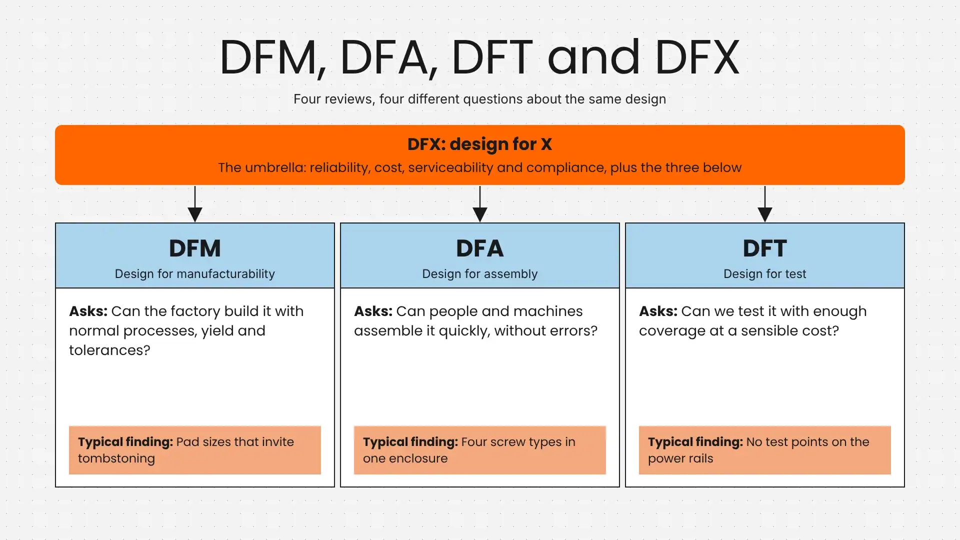
DFM, DFA and DFT ask different questions about the same design. Teams often use “DFM” for all of them, which is fine in conversation and unhelpful in a review request. Be specific.
| Term | Question it answers | Example finding |
|---|---|---|
| DFM (design for manufacturability) | Can the factory build this with its normal processes, yield and tolerances? | Pad sizes that invite tombstoning on small passives |
| DFA (design for assembly) | Can operators and machines assemble it quickly and without errors? | Four different screw types in one enclosure |
| DFT (design for test) | Can we test it with enough coverage at a reasonable cost? | No test points on the power rails |
| DFX (design for X) | The umbrella for all of the above, plus reliability, cost, serviceability and compliance | A connector that blocks access to the battery |
DFM and DFA are the pair people blur most often. DFM asks whether each part and process can be made reliably. DFA asks how the parts come together. A design can pass one and fail the other: a board that solders perfectly can still be impossible to fit into its enclosure.
Output. A prioritised list of changes, each tagged as must fix, should fix or worth considering.
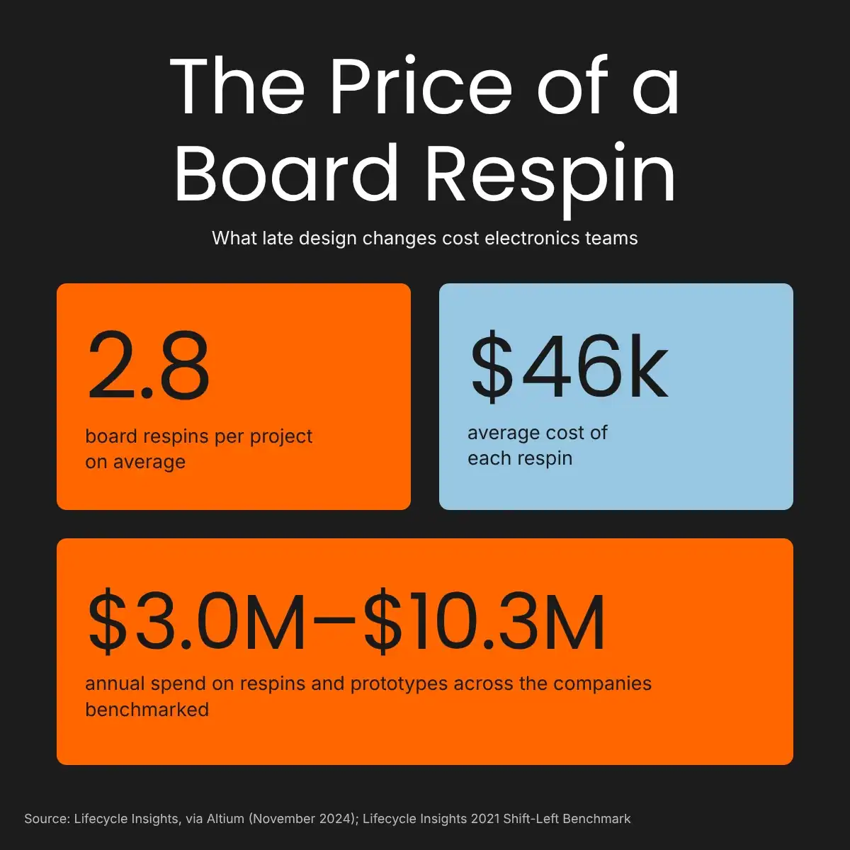
Nearly 60% of PCB designers produce just 1 to 5 respins a year. PCD&F / Circuits Assembly salary survey
Why design decisions lock in cost, yield and lead time
The design fixes most of what a product will cost to build, long before anyone buys materials. It sets the part count, the number of process steps, the test time, the yield and the lead time of the slowest component.
Changing it gets more expensive at every stage. On the screen, a change costs a conversation. After prototype boards, it costs a respin. After tooling, it costs a mould modification. After launch, it costs a field retrofit or a new revision.
Three things make late changes worse in electronics:
- Long lead times. A part swapped late may carry a lead time measured in months, not days.
- Coupled decisions. Moving one connector changes the board outline, the enclosure and the cable length at once.
- Validated builds. A change after DVT or PVT can mean repeating tests that took weeks.
That is why a DFM review is cheapest early and still worth running late. The NPI process builds it into the design stage for this reason.
Well over half of respondents (56%) cite late-stage design changes as a reason for missed dates.” Tech-Clarity research, via SOLIDWORKS
When to run a DFM review
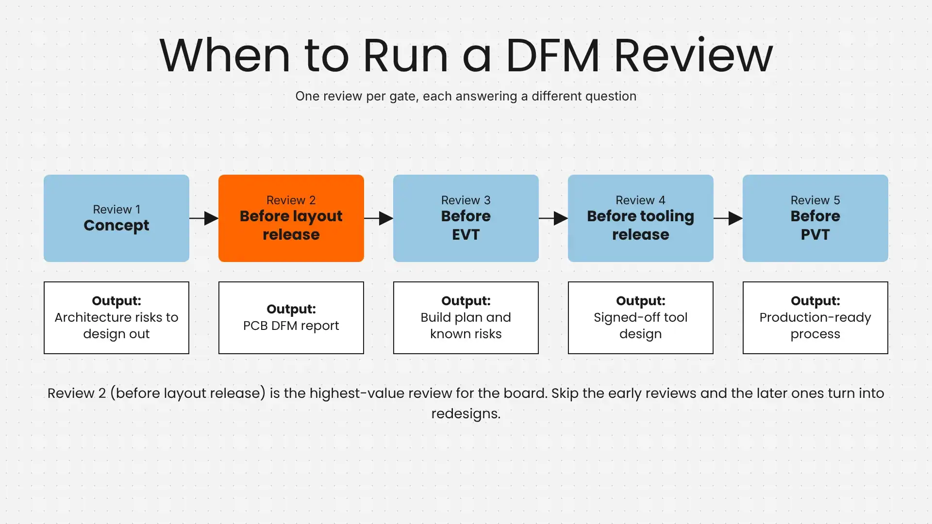
Run a DFM review at every stage, not once. Each stage asks a different question, and each is cheaper to answer before the next one starts.
- Concept and feasibility. Review architecture-level choices: component families, connectors, enclosure approach, battery and thermal strategy. Output: a short list of risks to design out.
- Before layout release. Review the schematic and BOM, then the PCB layout. This is the highest-value review for the board. Output: a PCB DFM report.
- Before EVT. Review the prototype build plan and process readiness. Output: confirmed build instructions and known risks.
- Before tooling release. Review the mechanical design for assembly and for moulding. Tooling changes after steel is cut are slow and costly. Output: a signed-off tool design.
- Before PVT. Review test fixtures, work instructions and line readiness. Output: a production-ready process, ready for PVT on the production line.
Each of these sits inside the wider NPI process, where DFM review is a defined stage with its own gate. Skip the early reviews and the later ones turn into redesigns.
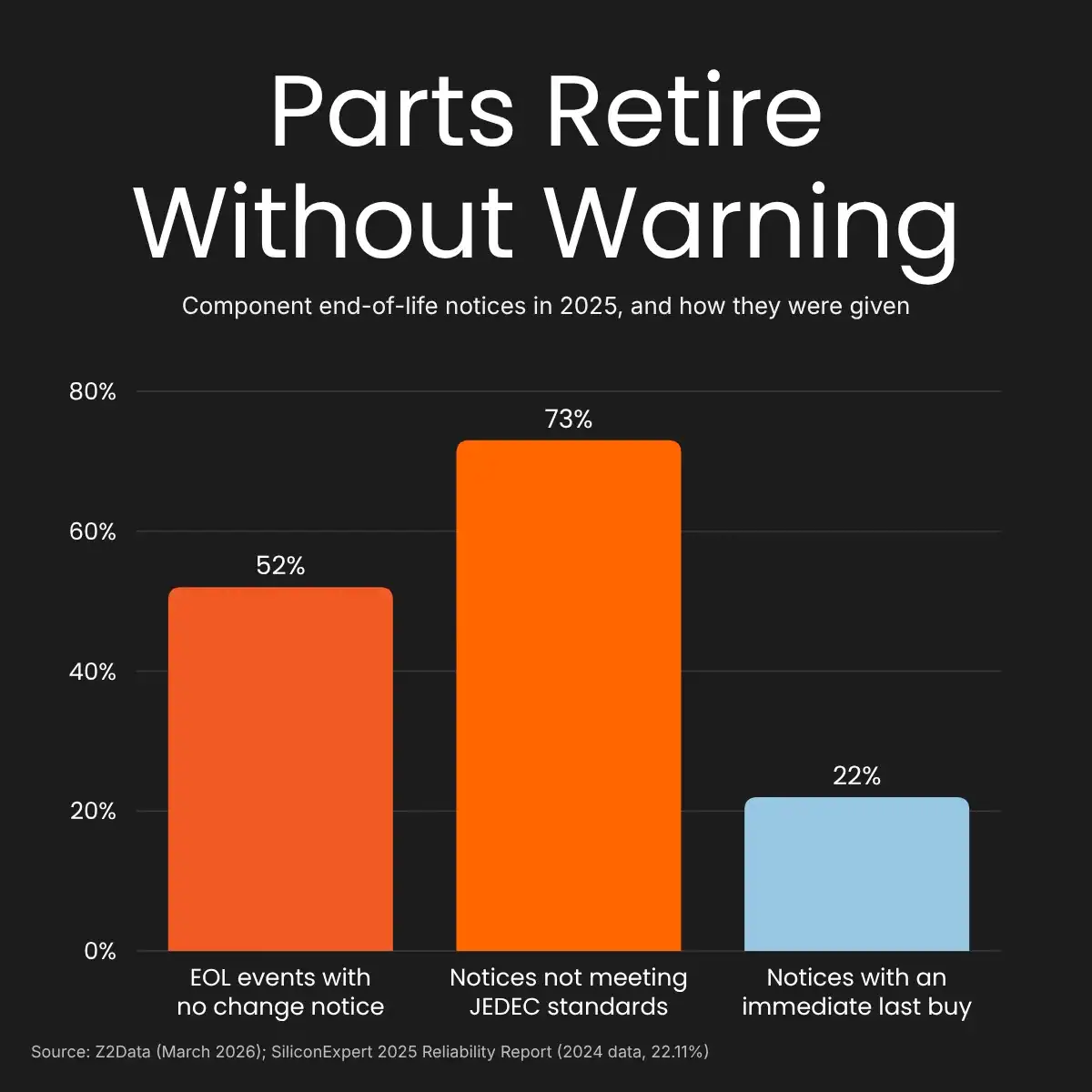
“111,150 components went obsolete without a PCN in 2023.” Converge, citing SiliconExpert data
PCB and PCBA DFM checklist
Start with the board. These checks catch the most problems before fabrication and assembly. Confirm every limit against your fabricator’s and assembler’s capability sheets, and work to standards such as IPC-2221 for generic PCB design, IPC-7351 for land patterns and IPC-2581 for data exchange, all published through the Global Electronics Association.
- Fabrication limits. Trace width and spacing, drill sizes and aspect ratio, annular rings, via-in-pad use, solder mask dams and copper-to-edge clearance, all within the fabricator’s stated capability. Specify impedance control together with the stackup.
- Panelisation. Design the array with rails, tooling holes and fiducials. Choose the depaneling method early, and keep parts clear of the break line.
Component placement. Leave space for pick-and-place and for rework. Keep polarity and pin 1 orientation consistent. Keep tall parts away from connectors and tool access. - Thermal and solder behaviour. Use symmetrical pad sizes on small passives to avoid tombstoning. Check paste volume on large thermal pads. Review the reflow profile for boards that mix heavy and light parts.
- Land patterns. Build footprints from verified libraries and check them against the datasheet. Keep silkscreen off pads.
- Fiducials and markings. Global and local fiducials for fine-pitch parts, readable reference designators and a revision mark on the board.
- Release package. Gerber, ODB++ or IPC-2581 files, a BOM with approved manufacturer part numbers, assembly drawings, a pick-and-place file, the stackup and any special instructions, all under revision control.
Output. A PCB DFM report with each finding marked must fix, should fix or consider.

“Our unpredictable world is turning typically reliable trends on their heads.” Steve Flagg, CEO and founder, Supplyframe
Design for assembly checklist: mechanical, cables and tolerances
DFA looks beyond the board to the product around it. Time and errors in final assembly come from mechanical decisions made weeks earlier.
- Part count. Every part is a purchase, a pick and a chance to fit it wrongly. Combine parts where function allows.
- Fastener variety. Use one or two screw types across the product. Prefer captive fasteners and snap-fits where the load allows.
- Assembly direction. Design so parts go in from one direction, top down, without turning the product over. Add self-locating features so parts align by shape, not by eye.
- Error-proofing. Make wrong assembly impossible with keyed connectors, asymmetric parts and features that block a reversed fit.
- Cables and connectors. Use board-to-board or blind-mating connectors where possible. Where cables remain, define length, routing channels and strain relief. Avoid flying leads.
- Tolerance stack-up. Check the combined tolerance of the PCB outline, connectors, standoffs and enclosure cut-outs. Parts that fit in CAD can fail to fit once tolerances stack.
- Access. Leave room for hands, tools and test probes. Check that you can fit and remove the last screw.
- Serviceability and rework. Decide which parts must be replaceable and make them reachable without removing others.
For the build that follows, see our guide to box build assembly.
Output. A DFA report that names each assembly step it expects to be slow or error-prone.

The median cost of engineering change orders is 10% of total new product development cost. APQC Open Standards Benchmarking
Design for test checklist
DFT is the cheapest insurance in the design. It costs a few test points and a header, and it decides whether you can find faults in seconds or not at all.
- Test points. Provide access to power rails, key signals, clocks and programming lines. Keep them on one side of the board where possible, with clearance for probes. Size and space them to suit both fixtures and flying probes.
- Programming and debug access. Add a header or pads for loading firmware, reachable with the board in its fixture. Plan how production firmware and serial numbers are written.
- Boundary scan. Where devices support JTAG boundary scan, route the chain and keep it accessible. It tests connections you cannot probe.
- Test modes in firmware. Build in commands that exercise outputs, read sensors and report status, so a functional test can drive the product without special hardware.
- Observable outputs. Make indicators and ports readable by the test system, with a defined way to confirm what the product is doing.
- Fixture features. Add alignment holes and keep-out zones for pogo pins, and avoid tall parts where the fixture needs to land.
- Data storage. Reserve memory for the serial number, calibration data and test status, so the unit carries its own record.
- Coverage target. Decide at design stage which faults the board test must find, then check the design provides access to find them.
For the methods these features support, see our guide to end of line testing.
Output. A test access plan that lists each test method, the points it needs and the coverage it delivers.
“Some 70% of all end-of-line defects are associated within the printing process.” SMART Group member poll, via Circuits Assembly
Components and BOM: lifecycle, second sources and packaging
A design is only manufacturable if its parts can be bought, in the right packaging, for the life of the product.
- Lifecycle status. Check every part’s status with its manufacturer: active, not recommended for new designs, or end of life. A part heading for end of life belongs in no new design.
- Second sources. Define approved alternates for critical and long-lead parts, and make sure footprint and function allow the swap. Where a part has no alternate, record it and plan for the risk.
- Lead time and allocation. Check current lead times before you commit. Prefer parts with several distributors and a stable supply history.
- Packaging. Specify tape-and-reel for machine placement. Cut tape and trays slow the line and raise cost.
- Moisture sensitivity. Record each part’s moisture sensitivity level (MSL) so storage, baking and exposure time are controlled on the line.
- Standardisation. Reuse parts across the range. Fewer unique part numbers mean larger purchase quantities and less stock risk.
- Manufacturer part numbers. Put approved manufacturer part numbers in the BOM, not generic descriptions, and keep them under revision control.
- Last-time buys. If a part reaches end of life, a last-time buy is a decision with a cost. Plan it as part of the product’s lifecycle, not as an emergency.
Output. A BOM review that flags each part by lifecycle, supply risk and alternate.
“Companies across sectors rate their digital maturity between one and two on a five-level scale.” Steve Flagg, Supplyframe
Enclosures and moulded parts: DFM for plastics
Moulded enclosures are where DFM mistakes get expensive, because the tool is steel and changes mean cutting metal. Review the design with a tooling engineer before release.
- Draft angles. Add draft to every face that releases from the mould, so parts eject cleanly without scuffing.
- Wall thickness. Keep walls as uniform as possible. Abrupt changes cause sink marks, warping and long cycle times.
- Ribs and bosses. Keep ribs thinner than the wall they support, and support screw bosses with ribs rather than making them thick.
- Gate and weld lines. Agree gate location early. Weld lines form where flow fronts meet and can weaken a part or mark a visible face.
- Snap-fits and clips. Design them within the material’s strain limits and allow for assembly forces, and for disassembly where service matters.
- Material choice. Choose a resin for strength, temperature range, flame rating (UL 94 where required) and finish. Check shrinkage and tolerance with your tooling team.
- Tolerances. Specify tight tolerances only on features that need them. Each one adds tooling effort and inspection time.
- Interfaces. Check the fit to the PCB, connectors, buttons, light pipes and seals using a tolerance stack-up.
Intretech’s advanced tooling team builds production moulds in house. Whichever partner you use, ask whether tooling engineers sit in the DFM review.
Common DFM mistakes and how a DFM review works with a partner
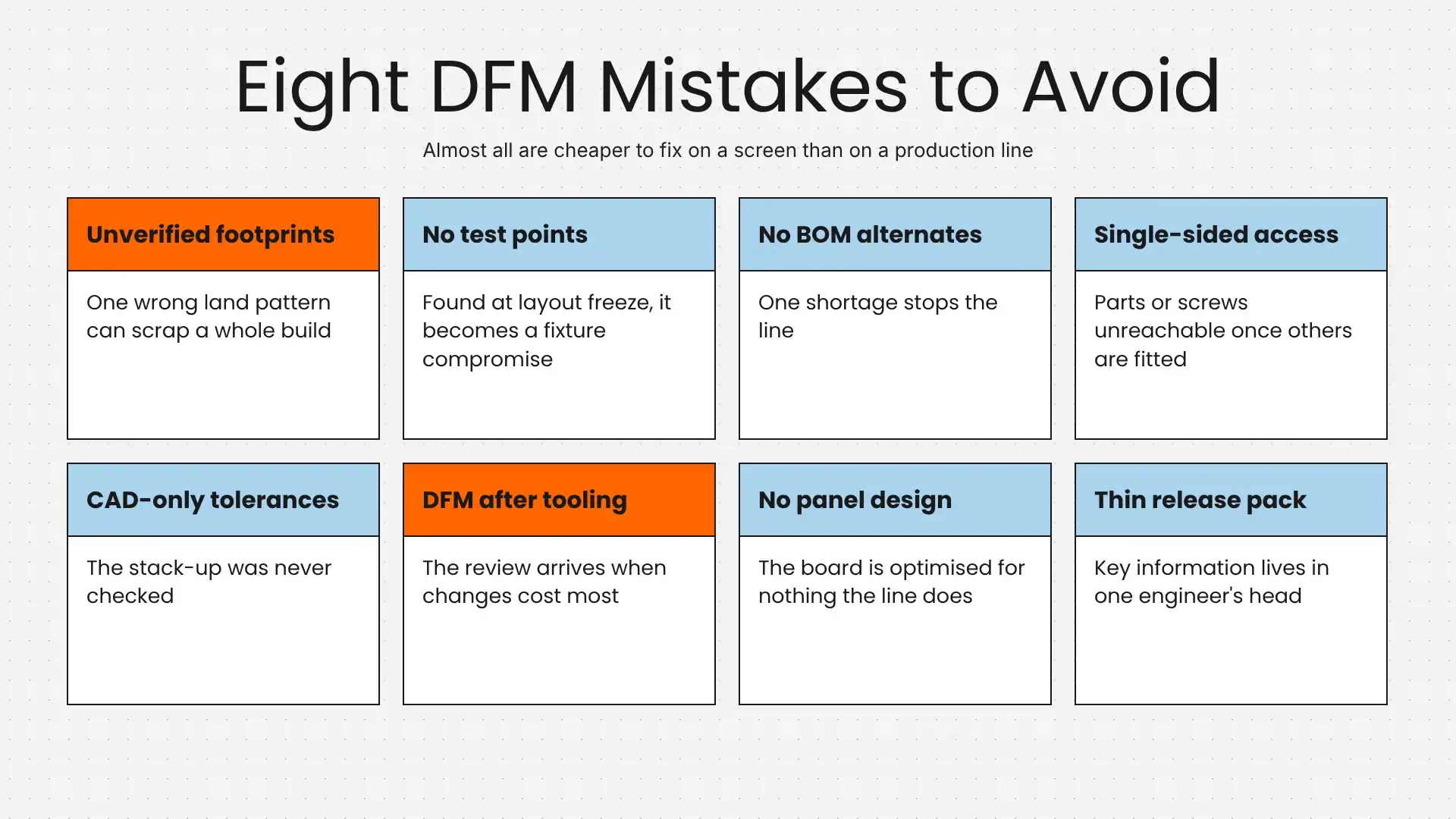
The same mistakes show up again and again.
- Footprints from unverified libraries. One wrong land pattern can scrap a whole build. Check each against the datasheet.
- No test points. Found at layout freeze, the gap becomes a fixture compromise.
A BOM with no alternates. One shortage stops the line. - Single-sided access. Parts or screws that cannot be reached once other parts are fitted.
- Tolerances that only work in CAD. The stack-up was never checked.
- DFM after tooling. The review arrives when changes cost the most.
- No panel design. The board is optimised for nothing the line actually does.
- An incomplete release package. Key information lives in one engineer’s head.
How a DFM review works with a design-and-manufacturing partner
A good review is a structured exchange, not a sign-off stamp.
- You send a complete package. Schematic, layout, BOM, mechanical files, test plan and target volume.
- The partner runs automated and engineering checks. Software finds rule violations. Process and tooling engineers review what software cannot, such as handling, access and moulding.
- You receive a report with severity. Each finding is marked must fix, should fix or consider, with the reason and a suggested change.
- You decide and respond. Some findings you will accept and some you will explain. Both are useful outcomes.
- The review repeats at each gate. Findings are closed out and new ones raised as the design matures.
This works best when design and manufacturing talk early and often. That is the case for joint design manufacturing, where the team that designs the product and the team that builds it share one process. At Intretech, our engineers lead DFM and test planning. Our article on connecting design with manufacturing performance explains the wider thinking.

Lead times were forecast to fall in Q4 2025 by 13.4% for passives and 5.3% for semiconductors. Supplyframe Commodity IQ (Nov 2025).
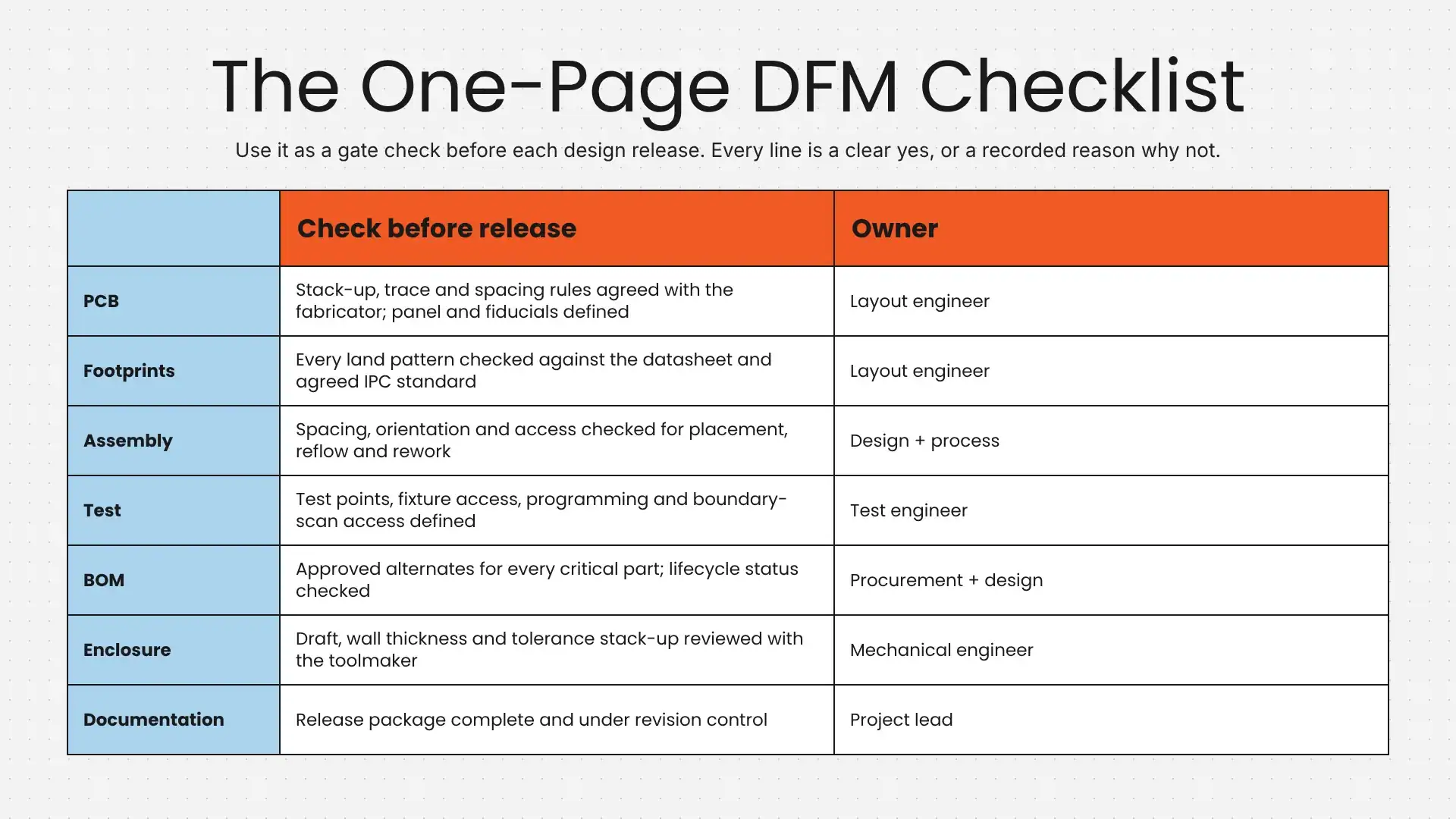
One-page DFM checklist summary
Use this as a gate check before each design release. Every line should be a clear yes, or a recorded reason why not.
|
Area |
Check before release |
Owner |
|---|---|---|
|
PCB |
Stack-up, trace and spacing rules agreed with the fabricator. Panel design and fiducials defined. |
Layout engineer |
|
Footprints |
Every land pattern checked against the datasheet and the agreed IPC standard. |
Layout engineer |
|
Assembly |
Component spacing, orientation and access checked for placement, reflow, handling and rework. |
Design and process engineer |
|
Test |
Test points on the board, fixture access planned, programming and boundary-scan access defined. |
Test engineer |
|
BOM |
Approved alternates listed for every critical part. Lifecycle status checked. |
Procurement and design |
|
Enclosure |
Draft angles, wall thickness and tolerance stack-up reviewed with the toolmaker. |
Mechanical engineer |
|
Fastening |
Screws, clips and connectors reachable in the actual assembly order. |
Mechanical and process engineer |
|
Documentation |
Release package complete: files, BOM, drawings, test plan, revision control. |
Project lead |
|
Review |
DFM findings logged with severity, decisions and close-out dates. |
Project lead |
Go deeper
Each topic in this checklist has a longer guide. For the build itself, read our guide to box build assembly. For test planning, see end of line testing for electronics. If you are building small quantities first, read about low volume manufacturing for electronics. For the wider process, see our NPI process and the breakdown of EVT, DVT and PVT.
Frequently asked questions
What is design for manufacturability in electronics?
Design for manufacturability (DFM) is the practice of designing a product so it can be built reliably, at the target cost and volume, with the processes a factory actually has. It covers the PCB, the components, the enclosure and the assembly sequence.
What is the difference between DFM, DFA and DFT?
DFM focuses on how individual parts are made. DFA focuses on how those parts go together. DFT focuses on how the finished product is tested. They overlap, and the best results come from running all three in the same review.
When should a DFM review happen?
As early as a first layout or mechanical concept exists, then again at each design gate. A review before tooling is released is the minimum. After tooling, the same finding costs far more to fix.
Who should do the DFM review?
The people who will build the product, together with the people who designed it. A review done only by the design team misses process constraints, and one done only by the factory misses design intent.
What files does a manufacturer need for a DFM review?
Schematic, PCB layout files, a complete BOM with manufacturer part numbers, mechanical models and drawings, the test plan and the target volume. The more complete the package, the more useful the findings.
Ready for a DFM review?
Explore more related content

The Top 3 Myths About JDM ODM OEM Explained
The Top 3 Myths About JDM ODM OEM ExplainedAsk three people in hardware what JDM, ODM and OEM mean and you'll often...

The 7 Steps of the Procurement Process: A Practical Guide for Manufacturing Teams
The 7 Steps of the Procurement Process: A Practical Guide for Manufacturing TeamsImportance of Procurement in Business...

Best Practices for Contract Lifecycle Optimization
Best Practices for Contract Lifecycle OptimizationMost contracts don't fail at signature. They fail six months later,...